Over the previous decade, one of many greatest tales in semiconductors has been a shock eclipsing of conventional silicon—within the subject of energy electronics, the place silicon carbide (SiC) and gallium nitride (GaN) have raced previous silicon to seize multibilllion-dollar segments of the market. And as main purposes fell to those upstarts, with their superior attributes, a query naturally arose. What could be the subsequent new energy semiconductor—the one whose superior capabilities would seize main market share from SiC and GaN?
Consideration has targeted on three candidates: gallium oxide, diamond, and aluminum nitride (AlN). All of them have exceptional attributes, in addition to basic weaknesses which have to date precluded industrial success. Now, nevertheless, AlN’s prospects have improved enormously due to a number of current breakthroughs, together with a technological advance at Nagoya College reported at the newest IEEE Worldwide Electron Gadgets Assembly, held this previous December in San Francisco.
How aluminum nitride edges as much as (and forward of?) SiC and GaN
The IEDM paper describes the fabrication of a diode primarily based on alloys of aluminum nitride able to withstanding an electrical subject of seven.3 megavolts per centimeter—about twice as excessive as what’s attainable with silicon carbide or gallium nitride. Notably, the system additionally had very low resistance when conducting present. “This can be a spectacular outcome,” says IEEE Senior Member W. Alan Doolittle, a professor {of electrical} and laptop engineering at Georgia Tech. “Significantly the on-resistance of this factor, which is ridiculously good.” The Nagoya paper has seven coauthors, together with IEEE Member Hiroshi Amano, who gained a Nobel Prize in 2014 for his function in inventing the blue LED.
“This can be a new idea in semiconductor units.” —Debdeep Jena, Cornell
Aluminum nitride has lengthy tantalized semiconductor researchers. One of the crucial essential traits of an influence semiconductor is its band hole. It’s the power, in electron volts, wanted for an electron within the semiconductor lattice to leap from the valence band to the conduction band, the place it’s free to maneuver round within the lattice and conduct electrical energy. In a semiconductor with a large bandgap, reminiscent of gallium nitride (GaN) or silicon carbide (SiC), the bonds between atoms are robust. So the fabric is ready to face up to very intense electrical fields earlier than the bonds break and the transistor is destroyed. However they each pale as compared with AlN. The bandgap of AlN is 6.20 electron volts; for GaN it’s 3.40 and for the most typical kind of SiC, 3.26.
One longstanding drawback with AlN is in doping, which is the insertion of impurity components that give a semiconductor an extra of prices, thereby enabling it to hold present. Methods for chemically doping AlN have solely begun rising lately, are usually not absolutely developed, and their effectiveness is a considerably contentious topic amongst researchers. In doping, the surplus prices might be electrons, during which case the semiconductor is known as “n-type,” or they are often electron deficiencies known as holes, during which case it’s “p-type.” Almost all commercially profitable units are made up of such doped semiconductors, sandwiched collectively.
However impurity doping, it seems, will not be the one strategy to dope a semiconductor. Some semiconductors primarily based on a compound containing components from group III (a.ok.a. the scandium group) and group V (vanadium group) within the periodic desk—for instance the compound gallium nitride—have an uncommon and noteworthy property. On the boundary the place two such semiconductors meet, they will spontaneously generate a two-dimensional pool of extraordinarily cellular cost carriers, known as a 2-dimensional electron gasoline, even with out chemical doping. It arises from an inside electrical subject within the crystal, which comes from a few attributes. For one, crystals of those III-V semiconductors are unusually polar: Throughout the unit cells of the crystal, the clouds of electrons and positively-charged nuclei are offset from one another sufficient to present each cell distinct damaging and optimistic areas (a dipole). As well as, it’s attainable to generate prices within the crystal lattice of those semiconductors just by straining that lattice, a phenomenon known as piezoelectricity.
The story behind the large advance
Within the early 2000s, researchers on the College of California, Santa Barbara exploited these traits to develop a method they known as distributed polarization doping, which allowed them to get n-type doping of bulk (three-dimensional) gallium-nitride with out impurity dopants. The group included IEEE Fellow Umesh Mishra (now dean of engineering at UCSB) and his graduate college students Debdeep Jena and Huili (Grace) Xing, each now at Cornell College. Jena and Xing, each IEEE Fellows, later demonstrated p-type distributed polarization doping, in 2010, after which dopant-free 2-dimensional gap gases, in 2018, at Cornell.
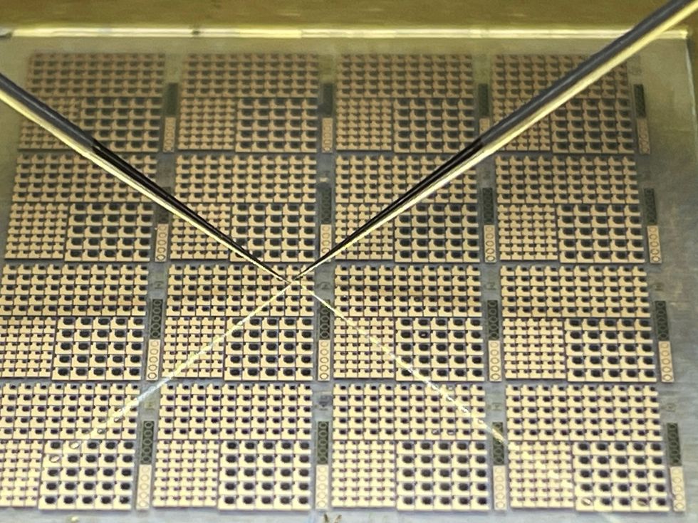 State-of-the-art aluminum nitride diodes are examined at Nagoya College.Nagoya College
The Nagoya group constructed on these prior achievements by implementing the strategy of dopant-free distributed polarization doping in aluminum nitride—or, extra exactly, an alloy of aluminum-gallium-nitride (AlGaN) consisting of a combination of AlN and GaN. Like all diode, their system has a p-doped area mated to an n-doped one, with a boundary, known as a junction, in between. For each areas, the doping was achieved with distributed polarization doping. They achieved the totally different polarizations, n-type and p-type, by establishing a gradient, in every of the doped areas, within the proportion of AlN vs. GaN within the alloy. Whether or not the doping is n-type or p-type relies upon merely on the course of the gradient.
“As an alternative of getting a uniform composition of AlGaN, the aluminum composition is altering spatially in a linear vogue,” says Jena. The p-doped layer begins off with pure gallium nitride on the aspect adjoining to the anode contact. Shifting in the direction of the junction with the n-doped layer, the proportion of aluminum nitride within the AlGaN alloy will increase, till it reaches 95 p.c AlN proper on the junction. Persevering with in the identical course, transferring via the n-doped area, the proportion of AlN falls off with distance from the junction, beginning at 95 p.c and bottoming out at 70 p.c AlN the place that layer makes contact with the pure AlN substrate.
The last word purpose is a commercially obtainable aluminum nitride energy transistor that’s enormously superior to the prevailing choices, and the Nagoya work has left little doubt that’s finally going to occur.
“This can be a new idea in semiconductor units,” says Jena, of the Nagoya system. The following step, he provides, is fabricating a diode that has a layer of pure AlN on the junction, quite than 95 p.c AlN. A layer of AlN simply two microns thick would suffice to dam 3 kilovolts, in accordance with his calculations. “That is precisely the place this may go within the very close to future,” he says.
At Georgia Tech, Doolittle agrees that there’s nonetheless room for big enchancment by incorporating larger ranges of pure AlN in future units. For instance, the breakdown electrical subject of the Nagoya diode, 7.3 MV/cm, is spectacular, however the theoretical most for an AlN system is about 15. Thermal conductivity, too, could be enormously improved with extra AlN. The power to conduct warmth is vitally essential for an influence system, and the thermal conductivity of the AlGaN alloy is mediocre—under 50 watts per meter-kelvin. Pure aluminum nitride, then again, could be very respectable at 320, in between GaN, at 250, and SiC, at 490.
The last word purpose is a commercially obtainable AlN energy transistor that’s enormously superior to the prevailing choices, and the Nagoya work has left little doubt that’s finally going to occur, in accordance with each Jena and Doolittle. “It’s simply engineering at this level,” says Doolittle. They each word that the Nagoya diode is a vertical system, which is the popular orientation for an influence semiconductor. In a vertical system, the present flows upward from the substrate on to contacts on the highest of the system—a configuration that enables most present circulation.
Not less than half a dozen AlN-based transistors have been demonstrated lately, however none of those have been vertical units and none had traits aggressive with commercially obtainable GaN or SiC transistors. They, too, relied on AlGaN in key elements of the system.
In an e-mail to IEEE Spectrum, IEEE Member Takeru Kumabe, a coauthor of the Nagoya paper, wrote, “we imagine it’s attainable to show commercially aggressive [power transistors] using distributed polarization doping expertise…. AlN-based vertical heterojunction bipolar transistors, which encompass two p–n junctions and exhibit good energy and space efficiencies, are our focused system, our dream, to be realized.”
Kumabe added that to comprehend that dream the group would deal with getting a deeper understanding of cost mobility, “provider lifetime, crucial electrical subject, and deep-level defects. Crystal-growth and device-fabrication applied sciences that produce high-quality system layers and introduce much less harm throughout processing must also be developed.”
“We need to resolve these factors inside 3-5 years and commercialize AlN-based energy units within the 2030s,” he stated.
From Your Web site Articles
Associated Articles Across the Net