In an unique interview forward of an invite-only occasion at present in San Jose, Intel outlined new chip applied sciences it is going to supply its foundry clients by sharing a glimpse into its future data-center processors. The advances embrace extra dense logic and a 16-fold enhance within the connectivity inside 3D-stacked chips, and they are going to be among the many first top-end applied sciences the corporate has ever shared with chip architects from different corporations.
The brand new applied sciences will arrive on the fruits of a years-long transformation for Intel. The processor maker is transferring from being an organization that produces solely its personal chips to turning into a foundry, making chips for others and contemplating its personal product groups as simply one other buyer. The San Jose occasion, IFS Direct Join, is supposed as a type of coming-out social gathering for the brand new enterprise mannequin.
Internally, Intel plans to make use of the mixture of applied sciences in a server CPU code-named Clearwater Forest. The corporate considers the product, a system-on-a-chip with lots of of billions of transistors, an instance of what different clients of its foundry enterprise will have the ability to obtain.
“Our goal is to get the compute to the perfect efficiency per watt we are able to obtain” from Clearwater Forest, stated Eric Fetzer, director of information middle expertise and pathfinding at Intel. Which means utilizing the corporate’s most superior fabrication expertise accessible, Intel 18A.
3D stacking “improves the latency between compute and reminiscence by shortening the hops, whereas on the identical time enabling a bigger cache”— Pushkar Ranade
“Nevertheless, if we apply that expertise all through your complete system, you run into different potential issues,” he added. “Sure elements of the system don’t essentially scale in addition to others. Logic usually scales era to era very properly with Moore’s Legislation.” However different options don’t. SRAM, a CPU’s cache reminiscence, has been lagging logic, for instance. And the I/O circuits that join a processor to the remainder of a pc are even additional behind.
Confronted with these realities, as all makers of modern processors are actually, Intel broke Clearwater Forest’s system down into its core capabilities, selected the best-fit expertise to construct every, and stitched them again collectively utilizing a collection of recent technical tips. The result’s a CPU structure able to scaling to as many as 300 billion transistors.
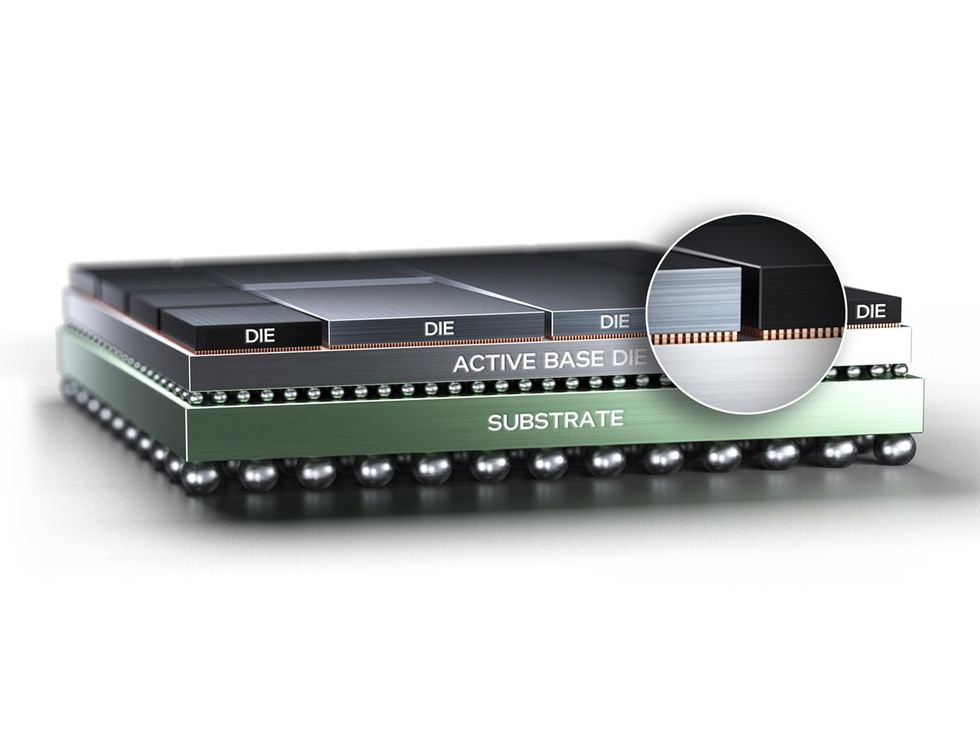
In Clearwater Forest, billions of transistors are divided amongst three several types of silicon ICs, referred to as dies or chiplets, interconnected and packaged collectively. The guts of the system is as many as 12 processor-core chiplets constructed utilizing the Intel 18A course of. These chiplets are 3D-stacked atop three “base dies” constructed utilizing Intel 3, the method that makes compute cores for the Sierra Forest CPU, due out this 12 months. Housed on the bottom die would be the CPU’s principal cache reminiscence, voltage regulators, and inside community. “The stacking improves the latency between compute and reminiscence by shortening the hops, whereas on the identical time enabling a bigger cache,” says senior principal engineer Pushkar Ranade.
Lastly, the CPU’s I/O system will probably be on two dies constructed utilizing Intel 7, which in 2025 will probably be trailing the corporate’s most superior course of by a full 4 generations. Actually, the chiplets are principally the identical as these going into the Sierra Forest and Granite Rapids CPUs, lessening the event expense.
Right here’s a have a look at the brand new applied sciences concerned and what they provide:
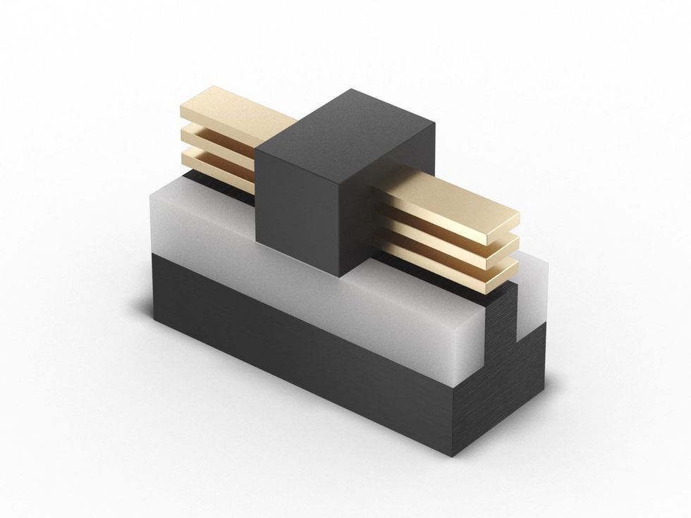
3D Hybrid Bonding
 3D hybrid bonding hyperlinks compute dies to base dies.Intel
Intel’s present chip-stacking interconnect expertise, Foveros, hyperlinks one die to a different utilizing a vastly scaled-down model of how dies have lengthy been linked to their packages: tiny “microbumps” of solder which are briefly melted to hitch the chips. This lets at present’s model of Foveros, which is used within the Meteor Lake CPU, make one connection roughly each 36 micrometers. Clearwater Forest will use new expertise, Foveros Direct 3D, which departs from solder-based strategies to carry a whopping 16-fold enhance within the density of 3D connections.
Referred to as “hybrid bonding,” it’s analogous to welding collectively the copper pads on the face of two chips. These pads are barely recessed and encompass by insulator. The insulator on one chip affixes to the opposite when they’re pressed collectively. Then the stacked chips are heated, inflicting the copper to increase throughout the hole and bind collectively to kind a everlasting hyperlink. Competitor TSMC makes use of a model of hybrid bonding in sure AMD CPUs to attach additional cache reminiscence to processor-core chiplets and, in AMD’s latest GPU, to hyperlink compute chiplets to the system’s base die.
“The hybrid bond interconnects allow a considerable enhance in density” of connections, says Fetzer. “That density is essential for the server market, notably as a result of the density drives a really low picojoule-per-bit communication.” The power concerned in information crossing from one silicon die to a different can simply devour an enormous chunk of a product’s energy finances if the per-bit power value is just too excessive. Foveros Direct 3D brings that value down under 0.05 picojoules per bit, which places it on the identical scale because the power wanted to maneuver bits round inside a silicon die.
Loads of that power financial savings comes from the info traversing much less copper. Say you needed to attach a 512-wire bus on one die to the same-size bus on one other so the 2 dies can share a coherent set of data. On every chip, these buses may be as slender as 10–20 wires per micrometer. To get that from one die to the opposite utilizing at present’s 36-micrometer-pitch microbump tech would imply scattering these indicators throughout a number of hundred sq. micrometers of silicon on one facet after which gathering them throughout the identical space on the opposite. Charging up all that additional copper and solder “rapidly turns into each a latency and a big energy downside,” says Fetzer. Hybrid bonding, in distinction, may do the bus-to-bus connection in the identical space that a number of microbumps would occupy.
As nice as these advantages may be, making the swap to hybrid bonding isn’t straightforward. To forge hybrid bonds requires linking an already-diced silicon die to 1 that’s nonetheless connected to its wafer. Aligning all of the connections correctly means the chip have to be diced to a lot larger tolerances than is required for microbump applied sciences. Restore and restoration, too, require completely different applied sciences. Even the predominant manner connections fail is completely different, says Fetzer. With microbumps, you usually tend to get a brief from one little bit of solder connecting to a neighbor. However with hybrid bonding, the hazard is defects that result in open connections.
Bottom energy
One of many principal distinctions the corporate is bringing to chipmaking this 12 months with its Intel 20A course of, the one that can precede Intel 18A, is back-side energy supply. In processors at present, all interconnects, whether or not they’re carrying energy or information, are constructed on the “entrance facet” of the chip, above the silicon substrate. Foveros and different 3D-chip-stacking tech require through-silicon vias, interconnects that drill down by means of the silicon to make connections from the opposite facet. However back-side energy supply goes a lot additional. It places all the energy interconnects beneath the silicon, basically sandwiching the layer containing the transistors between two units of interconnects.
 PowerVia places the silicon’s energy provide community under, leaving extra room for data-carrying interconnects above.Intel
This association makes a distinction as a result of energy interconnects and information interconnects require completely different options. Energy interconnects should be extensive to cut back resistance, whereas information interconnects needs to be slender to allow them to be densely packed. Intel is about to be the primary chipmaker to introduce back-side energy supply in a industrial chip, later this 12 months with the discharge of the Arrow Lake CPU. Knowledge launched final summer time by Intel confirmed that back-side energy alone delivered a 6 % efficiency increase.
The Intel 18A course of expertise’s back-side-power-delivery community expertise will probably be essentially the identical as what’s present in Intel 20A chips. Nevertheless, it’s getting used to larger benefit in Clearwater Forest. The upcoming CPU consists of what’s referred to as an “on-die voltage regulator” throughout the base die. Having the voltage regulation near the logic it drives means the logic can run sooner. The shorter distances let the regulator reply to modifications within the demand for present extra rapidly, whereas consuming much less energy.
As a result of the logic dies use back-side energy supply, the resistance of the connection between the voltage regulator and the dies logic is that a lot decrease. “The ability through expertise together with the Foveros stacking offers us a very environment friendly option to hook it up,” says Fetzer.
RibbonFET, the subsequent era
Along with back-side energy, the chipmaker is switching to a distinct transistor structure with the Intel 20A course of: RibbonFET. A type of nanosheet, or gate-all-around, transistor, RibbonFET replaces the FinFET, CMOS’s workhorse transistor since 2011. With Intel 18A, Clearwater Forest’s logic dies will probably be made with a second era of RibbonFET course of. Whereas the gadgets themselves aren’t very completely different from those that can emerge from Intel 20A, there’s extra flexibility to the design of the gadgets, says Fetzer.
 RibbonFET is Intel’s tackle nanowire transistors.Intel
“There’s a broader array of gadgets to assist numerous foundry functions past simply what was wanted to allow a high-performance CPU,” which was what the Intel 20A course of was designed for, he says.
 RibbonFET’s nanowires can have completely different widths relying on the wants of a logic cell.Intel
A few of that variation stems from a level of flexibility that was misplaced within the FinFET period. Earlier than FinFETs arrived, transistors in the identical course of may very well be made in a variety of widths, permitting a more-or-less steady trade-off between efficiency—which got here with larger present—and effectivity—which required higher management over leakage present. As a result of the principle a part of a FinFET is a vertical silicon fin of an outlined top and width, that trade-off now needed to take the type of what number of fins a tool had. So, with two fins you would double present, however there was no option to enhance it by 25 or 50 %.
With nanosheet gadgets, the flexibility to range transistor widths is again. “RibbonFET expertise permits completely different sizes of ribbon throughout the identical expertise base,” says Fetzer. “Once we go from Intel 20A to Intel 18A, we provide extra flexibility in transistor sizing.”
That flexibility signifies that commonplace cells, fundamental logic blocks designers can use to construct their techniques, can include transistors with completely different properties. And that enabled Intel to develop an “enhanced library” that features commonplace cells which are smaller, higher performing, or extra environment friendly than these of the Intel 20A course of.
2nd era EMIB
In Clearwater Forest, the dies that deal with enter and output join horizontally to the bottom dies—those with the cache reminiscence and community—utilizing the second era of Intel’s EMIB. EMIB is a small piece of silicon containing a dense set of interconnects and microbumps designed to attach one die to a different in the identical aircraft. The silicon is embedded within the bundle itself to kind a bridge between dies.
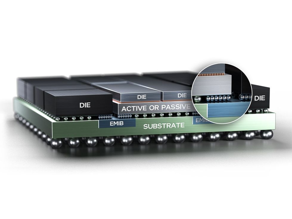 Dense 2D connections are fashioned by a small sliver of silicon referred to as EMIB, which is embedded within the bundle substrate.Intel
The expertise has been in industrial use in Intel CPUs since Sapphire Rapids was launched in 2023. It’s meant as a more cost effective different to placing all of the dies on a silicon interposer, a slice of silicon patterned with interconnects that’s giant sufficient for all the system’s dies to take a seat on. Other than the price of the fabric, silicon interposers will be costly to construct, as a result of they’re normally a number of occasions bigger than what commonplace silicon processes are designed to make.
The second era of EMIB debuts this 12 months with the Granite Rapids CPU, and it includes shrinking the pitch of microbump connections from 55 micrometers to 45 micrometers in addition to boosting the density of the wires. The primary problem with such connections is that the bundle and the silicon increase at completely different charges after they warmth up. This phenomenon may result in warpage that breaks connections.
What’s extra, within the case of Clearwater Forest “there have been additionally some distinctive challenges, as a result of we’re connecting EMIB on an everyday die to EMIB on a Foveros Direct 3D base die and a stack,” says Fetzer. This case, lately rechristened EMIB 3.5 expertise (previously referred to as co-EMIB), requires particular steps to make sure that the stresses and strains concerned are suitable with the silicon within the Foveros stack, which is thinner than odd chips, he says.
For extra, see Intel’s whitepaper on their foundry tech.
From Your Web site Articles
Associated Articles Across the Internet