There are various constraints on the design of augmented-reality methods. Not the least of which is that “it’s a must to look presentable whenever you’re strolling round,” Meta analysis scientist Tony Wu instructed engineers Tuesday on the IEEE Worldwide Strong State Circuits Convention (ISSCC). “You possibly can’t have a shoebox in your face on a regular basis.”
An AR system additionally have to be light-weight and may’t throw off plenty of warmth. And it must be miserly with energy as a result of no person needs to should recharge wearable electronics each couple of hours. Then once more, when you’ve received a flaming-hot shoebox in your face, you would possibly be glad about a brief battery life.
The 3D chip may observe two palms concurrently utilizing 40 p.c much less vitality than a single die may do with just one hand. What’s extra, it did so 40 p.c sooner.
Wu is a part of the Meta staff engaged on the silicon smarts to make an AR system, referred to as Aria, that’s as little like a scorching shoebox as they will make it. A giant a part of the answer, Wu instructed engineers, is 3D chip integration expertise. At ISSCC, Meta detailed how the corporate’s prototype AR processor makes use of 3D to do extra in the identical space and with the identical quantity or much less vitality.
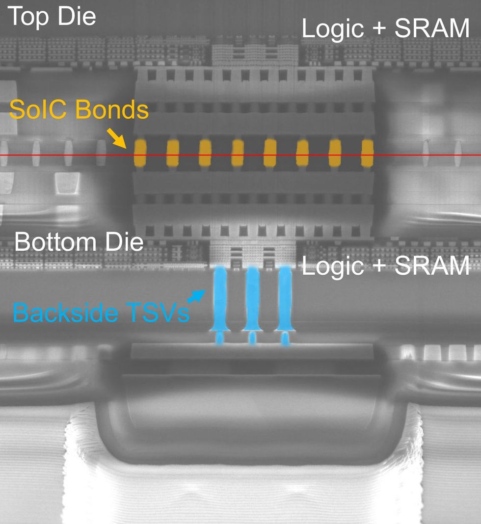 Meta’s prototype chip has each logic and reminiscence on every silicon die. They’re bonded face-to-face, and through-silicon vias carry knowledge and energy to each.Meta
The prototype chip is 2 ICs of equal dimension—4.1 by 3.7 millimeters. They’re bonded collectively in a course of referred to as face-to-face wafer-to-wafer hybrid bonding. Because the title implies, it entails flipping two absolutely processed wafers in order that they’re going through one another and bonding them so their interconnects hyperlink collectively instantly. (The “hybrid bonding” half means it’s a direct copper-to-copper connection. No solder wanted.)
The TSMC expertise used for this meant the 2 items of silicon may kind a vertical connection roughly each 2 micrometers. The prototype didn’t absolutely make use of this density: It required round 33,000 sign connections between the 2 items of silicon and 6 million energy connections. The underside die makes use of through-silicon vias (TSVs)—vertical connections bored down by way of the silicon—to get indicators out of the chip and energy in.
3D stacking meant the staff may enhance the chip’s computing energy—letting it deal with greater duties—with out including to its dimension. The chip’s machine-learning unit has 4 compute cores on the underside die and 1 megabyte of native reminiscence, however the prime die provides one other 3 MB, accessible by way of 27,000 vertical knowledge channels on the similar pace and vitality—0.15 picojoules per byte— as in the event that they had been one massive piece of silicon.
The staff examined the chip on a machine-learning job crucial for augmented actuality, hand monitoring. The 3D chip was capable of observe two palms concurrently utilizing 40 p.c much less vitality than a single die may do with just one hand. What’s extra, it did so 40 p.c sooner.
Along with machine studying, the chip can do image-processing duties. 3D made an enormous distinction right here, once more. Whereas the 2D model was restricted to compressed photos, the 3D chip can do full HD utilizing the identical quantity of vitality.
From Your Website Articles
Associated Articles Across the Net